LNW80 Technical Reference Manual
THEORY OF OPERATIONS
LNDOUBLER 5/8
The LNDOUBLER 5/8 has as its heart two floppy
controller IC's -- the FD1771 (single density controller) and
the FD1791 (single and double density controller). The
reason that the FD1771 is still needed is that the commands
are slightly different and the BOOT in the level II Roms
would not work. The two floppy controllers are tied
together so that only one of the two can be enabled at one
time.
SINGLE/DOUBLE DENSITY OPERATION
Single density operation is enabled when memory
location 37EC is written to with data FE. Double density
operation is enabled when memory location 37EC is written to
with data FF.
The controlling signals far single/double density
operation are DOUBLE* and DOUBLE, U16 pins 9 and 8
respectively. U5 and U6, open collector inverters, are tied
together to create an 8-input nor gate whose common output
is inverted through U7 and again through U12. U12-8 is used
to clock DAL0" into U16-12. Double density operation is
selected when DOUBLE and DOUBLE* are high and low
respectively.
The signal DOUBLE is input to U10-3, U11-1, and
U2-2. When U18-3 is low, the FD1771 is enabled. U11 is used
to select the STEP, DIRC, WD, and WG signals to be output to
the Floppy from either the FD1771 or FD1791. When U11-1 is
low the single density controller outputs will be selected.
U2 enables VFOE* (U2-3). This signal is input to the WD1691
and will be explained later.
The signal DOUBLE* is input, to U9-3, U9-37, and
U8-15. When U9-3 is low, the FD1791 is enab1ed. U9-37
enables the FD1791 for double density. And U8-15 enables
the WD1691 for double density.
CLOCK CIRCUIT
The LNDOUBLER 5/8 uses a series resonant circuit
utilizing Y1 and U12 to provide a 4MHz clock at U12-12.
This is then input to U14-13 which performs a divide by 2
result,in in a 2MHz clock at U14-5. Both the 4MHz and 2MHz
clocks are input to U13 pins 5 and 6 respectively. In 5.25"
operation the 2MHz clock is selected and then divided by 2
at U14 to become CLKI (U14-9) . In 8" operation the 4MHz
clock is selected and then divided by 2. CLKI is used to
clock both the FD1771 and the FD1791 pins 24, and is 1MHz in
5.25" operation and 2MHz in 8" operation.
5.25" & 8" SELECTION
On power up or reset, the LNDOUBLER 5/8 switches to
5.25" or 8" drive operation depending on the setting of the
5/8 switch.
When the 5/8 switch is in the 5 position, U17 will
be preset upon power up ox reset and the control signals
FIVE (U17-9) and FIVE* (U17-8) will go high and low
respectively enabling 5.25 operation. When the 5/8 switch
is in the 8 position U17 will be cleared upon power up or
reset and FIVE and FIVE* will go low and high respectively
enabling 8" operation.
5.25" and 8" operation may also be selected through
software switching. When memory location 37EE is written to
with data bits D7=1 and D6=1 the LNDOUBLER will switch to 8"
operation. When memory location 37EE is written to with
data bits D7=1 and D6=0 the LNDOUBLER will switch to 5.25"
operation.
5.25" & 8" OPERATION
FIVE* is input to U4-7 through R6 and determines the
pulse width of the one-shot used fox RDIN* (U4-12). In 8"
operation RDIN* has a pulse width of approximately 225us.
In 5.25" operation RDIN* has a pulse width of approximately
458 us.
FIVE is input to U13-1, an LS158, and is used to
select the various signals associated with either 5.25" or
8" operation.
The inputs to U13-3 associated with 5.25" operation
are a 2MHz clock (U13-6), a 2MHz voltage controlled
oscillator (U13-18), and gnd (U13-13).
The inputs to U13 associated with 8" operation are a
4MHz clock (U13-5), a 4MHz voltage controlled oscillator
(U13-11), and TG43MUX* (U13-14)
TG43 indicates that the RD/WR head is positioned
between tracks 44-76 and is valid only during RD and WR
commands. It is output from the FD1771 and FD1791 as STG43
and DTG43 respectively. STG43 and DTG43 are then inverted
through U5, an open collector inverter, and the outputs are
tied together producing TG43MUX*. In 5.25" operation TG43
is always enabled. In 8" mode TG43 is enabled only for
tracks 44-76.
ANALOG PHASE LOCK LOOP DATA SEPARATION
U15, an LS629, provides the VCO, voltage controlled
oscillator frequency of 4MHz (2MHz for 5.25" operation) for
the WD1691. (U8). In order to guarantee that it is not
sensitive to power supply variations, VRl (78L05) provides a
regulated supply to the LS629 and the adjustment controls
R25 and R26. R25 is a multiturn pot to adjust the frequency
range and R26 adjusts the bias voltage for the VCO. The
WD1691 and the 74LS629 make up the ANALOG PHASE LOCK LOOP
DATA SEPERATION. Far further details refer to the data
sheets supplied in this manual.
PRECISION WRITE PRECOMPENSATION
The WD2143 provides an accurate write
precompensation value according to the adjustment of R24. A
negative true pulse of the actual precompensation value can
be observed with an oscillcscepe at U8-4. Write
precompensation is factory aligned to 200ns +/- 25ns and is
enabled only for double density operation (all tracks 5.25"
and tracks above 43 for 8"). For further details of the
interface between the WD2143 and the WD1691 refer to the
data sheets.
WAIT LOGIC
The "wait" logic circuitry consists of U1, U2, U6,
U7, and U18.
The "wait" logic allows 8" disk dxive operation
under a slow CPU speed. This logic is used by several
operating systems and is maintained for compatibility
reasons.
When the memory location 37EE is written to with
data bits D7=1 and D5=1 then the "wait" logic is turned on.
When memory location 37EE is written to with data bits D7=1
and D5=0 then the "wait" logic is turned off.
Although the "wait" logic need not be invoked for
single density operation for 8" drives at the 1.77MHz CPU
speed an explanation of its operation follows:
1. The "wait" logic is turned on
2. The FDC is initialized and registers set
3. The command is given to the FDC to read
or write
4. The status register is read causing the
"wait" logic to issue a "wait" to the CPU
until:
a. the busy bit in the status register
goes false
b. DRQ on the FDC goes true
c. IRQ en the FDC goes true
If the condition that removed the "wait" was (a) or
(b) then the "wait" logic is still "on" but the CPU wait was
removed until the next time the status register of the FDC
is read. If the condition that turned off the wait was (c)
then the wait logic is turned off.
TROUBLESHOOTING
It is not within the scope of this manual to provide
a complete and detailed procedure for troubleshooting the
LNW80. But for those with technical experience in digital
electronics, this section may provide some helpful hints.
POWER SUPPLY
The first step in troubleshooting is to check the
supply voltages. The following voltages should be verified
at the corresponding test point.
REGULATED VOLTAGE TEST POINT
+5v +/- .3V JP1;JP3;JP5
+12V +/- .5V JP9
-12V +/- .5V JP7
-5V +/- .3V JP11
Note that the -5V supply is critical to the RAM's.
If it is not present damage may occur to those parts.
Therefore check the -5V supply first. If it is not present
then disconnect the other supplies before troubleshooting
further.
If the fuses continually blow you may disable the
overvoltage protection by removing the SCR's. But before
doing so disconnect the power supplies. Be ready to turn
off power if any component begins smoking.
VIDEO OUTPUT/ADJUSTMENTS
After the power supplies have been verified proceed
to check that there is a video output. If there is a video
output but it seems unstable or out, of sync, then try
adjusting C148. If that doesn't work then check the video
divider chain noting in particular the horizontal and
vertical sync pulses. If there is no video, then first
check for sync pulses. If all the sync pulses seem correct
then check the alphanumeric and graphic shift registers.
Keep in mind that the CPU may be instructing the VIDEO to
clear the screen.
SYSTEM CLOCK
Check that the Z80A has a clock at U2-6. If not
then follow the circuitry back to find out why. It should
be either 4MHz (high speed) or 1.77MHz (low speed) .
CPU/CPU TEST
There is a method by which you may test the RAM,
BASIC ROM, VIDEO RAM, and KEYBOARD. This procedure requires
two computers. One must be a known good 16K level 2 TRS80
or 16K LNW80.
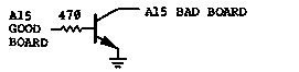
A special cable must be created in which A15 is
inverted from the good board to the bad board to enable the
good board to take over control. By doing so the bad board
will be perceived by the good to occupy the upper 32K of
memory space.
SPECIAL CABLE
Materials:
40 pin cable, 2N3906 transister, 478 ohm resiser
Procedure:
Break lines 7 and 8 on the cable. Line 7 corresponds
to pin 8 on the connector and line 8 corresponds to pin 7 en
the connector. Pin 8 is ground and pin 7 is A15. Connect
pin 8 from the good beard to the emitter of the transistor.
Connect pin 7 from the good board through a 470 ohm resister
to the base of the transister. And connect the collector to
pin 7 of the bad board. Connect the two computers together
and chm out the connections to verify proper connection.
 ENABLING THE BUS
If the bad board was preassembled by LNW RESEARCH
then no further modificatiens must be made except pulling
U2-25 to ground and reducing noise on the MUX line by
placing a parallel combination of a 100 ohm resister and a
330 pf capacitor from U18-5 to ground.
If the bad board was purchased as a bare board and
built as a kit then the following modifications must also be
made: lift the pins of U36-3 and U46-5; jumper U36-12 to
U18-7, U18-9 to U18-3.4, and U18-5 to U18-15.
Erratum #2 10-22-82
Break line 24 of the cable, Line 24 corresponds to
pin 23 of the connector. This prevents the good
computer from being disabled when U2-25 of the bad
board is pulled to ground.
CPU TO CPU TEST PROGRAM
5 CLS:PRINT"CPU TO CPU TEST":PRINT:PRINT:PRINT
10 INPUT"TEST ROM,RAM,VID,KEY";ZX$
20 IF ZX$="ROM" THEN 100 ELSE IF ZX$="RAM" THEN 200
ELSE IF ZX$="VID" THEN 300 ELSE IF ZX$="KEY" THEN 400
30 GOT010
100 INPUT "SELECT ROM NUMBER(A,A1,B,C1,ALL,LOOP)"; ZX$
105 C=-32767
110 IF ZX$="A" THEN 120 ELSE IF ZX$="A1" THEN 121 ELSE
IF ZX$="B" THEN 122 ELSE IF ZX$="B1" THEN 123 ELSE
IF ZX$="C" THEN 124 ELSE IF ZX$="C1" THEN 125 ELSE
IF ZX$="ALL" THEN 126 ELSE IF ZX$="LOOP" THEN 127
ELSE 10
120 Y=0:GOT0150
121 Y=2048:GOT0150
122 Y=4196:GOT0150
123 Y=6144:GOT0150
124 Y=8192:GOT0150
125 Y=10240:GOT0150
126 FOR X=-32767 TO -20480: IF PEEK (X)=PEEK(Y) THEN 130
ELSE 140
127 INPUT"LOCATION DESIRED(DECIMAL 0-12287) ";Z:LET
Z=Z-32768
128 ?PEEK (Z):GOT0128
130 ?Y: Y=Y+1:NEXTX:PRINT "TEST COMPLETE":GOTO10
140 PRINT"TEST FAILED":PRINT"LOC. EXPECTED ACTUAL":
PRINT Y,PEEK(Y),PEEK(X):Y=Y+l:STOP:NEXTX
150 A=Y+C:B=A+2047:FOR X=A TO B:IF PEEK (X)=PEEK(Y) THEN 130
ELSE 140
151 ?Y:Y=Y+Z:NEXTX:?"TEST COMPLETE":GOTO10
200 Y=170: FOR X=-16384 TO -1: POKE X, 170: IF PEEK(X)=170 THEN
NEXT X ELSE 220
210 Y=85:FOR X=-16384 TO -Z:POKE X,85:IF PEEK(X)=85 THEN
NEXT X ELSE
225 ?"TEST COMPLETE":GOT010
220 ?"TEST FAILED":?"LOC. EXPECTED ACTUAL":
? X+32768,Y,PEEK(X):STOP:NEXTX
300 Y=0:FOR X=-17408 TO -16385:?X+32767:POKEX,Y:Y=Y+1:
IFY=192 THEN
302 NEXTX
310 Y=0:FOR X=-17408 TO -16385:?X+32767: Z(3)=0:GOSUB600:
IF Z(1)=Y THEN 320 ELSE 350
320 Y=Y+X:IF Y=192 THEN
322 NEXTX:?"TEST COMPLETE":GOTO10
350 ?"VIDEO RAM FAILED TEST":?"LOC, EXPECTED ACTUAL":
?X+32768,Y,PEEK(X):Y=Y+l:IF Y=192 THEN Y=0
353 NEXT X:?"TEST COMPLETE":GOTOZ0
400 ?PEEK(-18177):G0T0400
600 Z(3)=Z(3)+1:Z(1)=PEEK (X):Z(2)=PEEK(X):IF Z(1)=Z(2)
THEN RETURN ELSE IF Z(3)=25 THEN RETURN ELSE 600
CPU/CPU TEST PROGRAM
The previously listed program will enable you to
test the program RAM, ROM, LORES VIDEO RAM, and KEYBOARD on
the "bad" board. Remember that the bad board will be
perceived by the good board from locations 32768 to 65535.
Remember also that writing to or reading from the upper 32K
requires that you use negative numbers. The following is a
simple formula for translating the actual location to the
location to be poked to peeked:
POKE OR PEEK ADDDRESS = ACTUAL ADDRESS - 32768
The simplest procedure for loading this program is
to type it in and save to cassette. This will prevent, you
from having to retype it, if the system crashes. Connect the
two computers together, power up the good board and load
level 2 basic. Then load the program from cassette and then
turn on the power on the bad board. The program will not
load if the power to the bad board is already on.
The program will display a simple menu. Respond
with ROM and the program will ask you whether you wish to
test ROM A1, A, B1, B, C1, C, or all. You may also loop on
any one location. The way the ROM test works is that it
pecks the same location on both the good and the bad board
and compares. Note that if you are using a TRS80 as your
"good" board then some of the ROM locations will disagree.
You may continue by typing "CONT".
The RAM part of the CPU test pokes data=170 to all
16K of the program RAM and peeks those locations to verify.
Then data is set equal to 85 and the process repeats itself.
These values are selected because they represent two
patterns of alternating "ones" and "zeros" in binary. The
entire RAM test takes about 5 minutes. Upon completion the
program will respond with "TEST COMPLETE".
The video part of the CPU test first writes to every
location. You may observe this by connecting the CRT to the
bad board. Afterwards it reads back to verify that the
correct information was stored. An occasional error may
occur due to noise. A good signal to loop on while
accessing the video memory is "CPUACC"" (U139-1).
The KEYBOARD part, of the CPU test will loop
continuously peeking a keyboard address. For this part of
the test you must connect a kybd to the "bad" board. With
no keys depressed zero's should be displayed on i,he CRT.
When a key is depressed the value displayed should
correspond to a "1" at the data bit which corresponds to
that particular key. Refer to the kybd schematic. To
escape the KYBD test you must depress the break key on the
"good" board.
If there is a failure you may loop at the location
of the failure and trigger on the appropiate enabling signal
to verify that the data and address are correct. Two sample
programs are:
1 A=PEEK (-32768):GOTO1
1 POKE -16384,0:GOT01
The 1st program will loop on a read of the 1st location of
ROM. The 2nd will loop on a write to the 1st location of
RAM with data equal to zero. In the 1st case you should
trigger on ROMRD* (U66-6). In the 2nd case, trigger on CAS*
(U96-15).
If you have verified that the ROM, RAM, VID RAM, and
KYBD sections are good then you may assume that the problem
is in the CPU section. All you can do is check to see that
all the control lines, address lines, and data lines are
functioning. If the CPU is "hanging up", ie. getting locked
on a RD*, you may "trick" it by lifting the RD* and NREQ*
lines on the Z80A.
"SCOTCH TAPE TRICK"
Sometimes the CPU/CPU test will not work because
connecting to the "bad" beard causes the good board to
hang-up. An example of this would be if any of the critical
bus lines were shorted. You may be able to determine which
line or lines are causing the problem by covering the 40 pin
connecter with scotch tape and removing it pin by pin. If
removing the scotch tape from a pin causes the good beard to
hang-up then you may assume that something is either shorted
to that line, driving that line, or possibly loading that
line down.
HI RESOLUTION GRAPHICS
The HRES GRAPHICS can be tested by running the HRES
GRAPHICS TEST on the following page. If the program fails
you must troubleshrot the associated circuitry. There is no
easy way to loop on the HRES GRAPHICS RAM to see if the
address and data are correct. You may allow the test
program to continue without stopping by deleting line 220.
While the program is running you can check the signals with
an oscilloscope to see that they are active. If the
program
is writing to two or more lines at a time you may assume you
have an addressing problem. If no data is being written
check the write line. If after running, the CRT does not
display an eighty character screen check HRES (55-5). If
the test does not fail but the information en the screen
seems incorrect check the shift register at U127.
10 REM HIGH RESOLUTION GRAPHICS TEST
20 REM CASSETTE VERSION
30 CLS
40 PRINT"LNW RESEARCH HRES GRAPHICS TEST"
50 FOR Z=0 TO 1000
60 NEXT Z
70 OUT 254,2
80 FOR X=32512 TO 32533
90 READ D
100 POKE X,D
110 NEXT X
120 POKE 16526,0:POKE 16527,127
125 LET Y=X
130 FOR Z=H TO 4
140 REM NOW POKE DATA TO BE OUTPUT TO USR ROUTINE
150 POKE 32522,Y
155 GOSUB 170
160 LET Y=Y*2
161 NEXTZ
162 LET Y=0
166 POKE 32522,0
167 GOSUB 170
168 PRINT "ALL MEMORY LOCATIONS TESTED"
169 END
170 FOR X=0 TO 16383
180 A=USR (X)
190 LET A=A AND 63
200 IF A=Y THEN GOTO 238
205 PRINT"MEMORY LOCATION FAILED TO READ OR WRITE
CORRECTLY"
207 PRINT"ADDRESS EXPECTED DATA ACTUAL DATA"
210 PRINT X;Y;A
220 STOP
230 NEXT X
240 RETURN
270 DATA 205,127,10,219,254,246,8,211,254,54,0,0,110,38,0
280 DATA 238,247,211,245,195,154,10
COLOR GRAPHICS TEST AND ADJUSTMENTS
1.Run "COLOR BAR TEST PROGRAM" and wait for it to complete.
2.Measure the voltage at pin 6 of U146. Record this value,
it should be between 1.25 and 1.75 volts.
3.While measuring the voltage at pin 5 of U146 adjust R99
so
that the voltage is the same as the recorded value.
4.While measuring the voltage at pin 7 of U146 adjust R98
so
that the voltage is the same as the recorded value.
5.Adjust R94 for best picture.Note that this effects the
luminance level and be observed at pin 9 of U146. The
observed level should be between .75 and 1.1 volts.
10 REM COLOR BAR TEST PROGRAM
20 REM CASSETTE VERSION
30 REM THIS TEST SHOULD GENERATE THE FOLLOWING COLORS:
35 REM WHITE GREEN YELLOW RED MAGENTA BLUE BLUE-GREEN BLACK
36 CLS:PRINTCHRS(23)
40 PRINT LNW RESEARCH COLOR BAR TEST"
45 REM DELAY BEFORE STARTING TEST
50 FOR Z=0 TO 1000
60 NEXT Z
70 OUT 254,4
72 FOR X=15368 TO 16383
74 POKE X,255
76 NEXT X
80 FOR X=32512 TO 32533
90 READ D
100 POKE X,D
110 NEXT X
120 POKE 26526,8:POKE 16527,127
125 FOR X=0 TO 12288
130 FOR Y=0 TO 7
135 FOR Z=0 TO 7
150 POKE 32522,Y+9
180 A=USR (X)
190 LET X=X+1
280 NEXT Z
220 NEXT Y
220 LET X=X-1
230 NEXT X
240 END
270 DATA 205,127,10,229,254,246,8,211,254,54,0,0,110,38,0
280 DATA 230,247,211,254,195,154,10
TROUBLE-SHOOTING THE EXPANSION INTERFACE
If connecting the expansion interface to the main
computer board causes the system to lock up refer to the
"SCOTCH TAPE TRICK" in the previous section.
POWER SUPPLY
As stated previously, the first step in
trouble-shooting is to verify the power supply. So proceed
to verify the following voltages at the following reference
points:
REGULATED VOLTAGE TEST POINT
+5V +/- .3V JP2,JP4
+12V +/- .5V JP12
-12V +/- .5V JP10
-5V +/- .3V JP8
Note that the -5V supply is critical to the RAMs.
If it is not present damage may occur to those parts.
32K MEMORY EXPANSION
The same procedure as used in the CPU/CPU TEST may
be used to trouble-shoot the additional 32K of program
memory. A sample program to test the memory is:
10 Y=170
20 FOR X=-32767 TO -1
30 POKE X,Y
40 A=PEEK(X)
50 IF A=Y THEN NEXT X ELSE 60
51 Y=85:Z=Z+1:IF Z=2 THEN 55 ELSE 20
55 PRINT"TEST COMPLETE":STOP
60 PRINT"LOCATION "X+65536;"ACTUAL",A;"EXPECTED",Y
70 STOP
80 NEXTX
Before running this program "set" the memory size to
32767. This will prevent the program from being stored in
the upper 32K of memory. If there is a failure you may PEEK
or POKE at that location using a simple loop statement. By
triggering on CAS* you may verify that the correct address
and data are present. Remember that the following
relationship exists between the actual location and that
poked or peeked:
ACTUAL ADDRESS = POKE OR PEEK ADDRESS + 65536
FLOPPY DISK CONTROLLER
If the FDC is not working, check that the 1MHz clock
input to U14-24 is present. Check that when reset MR*
(U14-19) goes low. If the motor on the drive does not go
on, or if it stays on continuously then the problem may be
related to U19 or U7. Note that if the motor stays on
continuously the problem is likely to be a reversed floppy
cable. By looping on POKE and PEEK statements and checking
with an oscilloscope you may verify that the decoder at U19
is operating correctly. Follow the interupt logic from
U14-39 to U1-6. Verify that U13 is selecting drive 0 and
that U14-23 goes high indicating that the status register is
ready. Check the gates of U1, U2, and U6 to see that
they're inverting their inputs. Remember that these are
7438's (open collector) and that the outputs must be pulled
up by the disk drive.
RS232 HANDSHAKING
To test the handshaking short the following points
together on J2:
J2-4 to J2-5 to J2-6
and J2-8 to J2-20 to J2-22
Load the following program:
10 FOR Y=0 TO Y=3:OUT234,Y:A=INP(232)
20 PRINT "Y=";Y, "A=";A:NEXTY
30 PRINT"FOR Y=0, A SHOULD BE 0000XXXX BINARY"
40 PRINT"FOR Y=1, A SHOULD BE 1100XXXX BINARY"
50 PRINT"FOR Y=2, A SHOULD BE 0011XXXX BINARY"
60 PRINT"FOR Y=3, A SHOULD BE 1111XXXX BINARY"
This program latches data through U26 and back again
through U33. OUT234 clocks the data out through U26 and
INP(232) clocks it back through U33. Refer to the
schematics.
RS232 SEND/RECEIVE
To test or troubleshoot the send/receive functions
of the RS232 port load the SERIAL CRT TERMINAL PROGRAM and
short E1 to E3. If the serial port is functioning properly
then as letters are typed on the keyboard they are routed
out through E3 and then back again through E1 and placed on
the CRT. If this is not occuring then check U40-25 to see
if data is being passed out through the UART. If so then
10 REM SERIAL CRT TERMINAL PROGRAM-CASSETTE VERSION
20 REM
30 REN THIS PROGRAM ALLOWS THE USE OF THE LNW SYSTEM
40 REM EXPANSION CIRCUIT BOARD AS A CRT TERMINAL. THIS
50 HEM PROGRAM MAY ALSO BE USED FOR TESTING THE SERIAL
60 REM INTERFACE BY SHORTING El AND E3 TOGETHER
65 REM
70 FOR X=28672 TO 28764
80 READ D
90 POKE X,D
100 NEXT X
110 POKE 16526,8
120 POKE 16527,112
130 A=USR (N)
200 DATA 62,28,205,51,0,62,31,205,51,0,62,14,205,51,0,211
210 DATA 232,219,233,230,248,246,5,211,234,219,234,203,127
220 DATA 40,23,219,235,183,40,18,230,127,254,96,250,45,112
230 DATA 230,95,254,10,40,232,205,51,0,24,227,205,43,0,183
240 DATA 40,221,254,5,242,73,112,33,88,112,79,6,0,9,126
250 DATA 254,26,40,204,79,219,234,203,119,40,249,121,211
260 DATA 235,24,192,3,27,124,127
10 REM SERIAL PRINTER DRIVER PROGRAM-CASSETTE VERSION
20 REM
30 REM THIS PROGRAM ALLOWS THE USE OF A SERIAL PRINTER
40 REM WITH THE LNW RESEARCH SYSTEM EXPANSION CIRCUIT
50 REM BOARD. THIS DRIVER PROGRAM IS LEFT IN MEMORY AT A
60 REM LOCATION WHICH IS UNALTERED BY BASIC AND BY USER
70 REM PROGRAMS. THE PROGRAM IS EXECUTED DURING EVERY
80 REM LPRINT AND LLIST FOR EACH CHARACTER TO BE PRINTED
90 REM HANDSHAKING IS SUPPORTED AS THE SOFTWARE READS
100 REM THE PRINTER BUSY (DSR) BEFORE OUTPUTING A
110 REM CHARACTER. NOTE: IN ORDER FOR THIS PROGRAM TO BE
120 REM EXECUTED, THE LINE PRINTER CONTROL BLOCK AT HEX
130 REM 4025 TO 4027 MUST BE ALTERED BEFORE PRINTING TO
140 REM IDENTIFY THE PRINTER TYPE AND DRIVER ADDRESS.
150 REM THE FOLLOWING LIST GIVES YOU THESE VALUES.
160 REM 16421D 4025H DCB TYPE02H 002D
170 REM 16422D 4026H LSB DRIVER ADDR. 00H 000D
180 REM 16423D 4027H NSB DRIVER ADDR. 7FH 127D
190 REM
200 FOR X=32512 TO 32560
210 READ D
220 POKE X,D
230 NEXT X
240 POKE 16526,8
250 POKE 16527,127
260 A=USR (N)
300 DATA 245,58,48,127,254,1,40,15,62,1,50,48,127,211,232
310 DATA 219,233,230,248,246,4,211,234,241,219,232,203,119
320 DATA 32,250,121,211,235,254,13,32,4,14,10,24,233,200,0
proceed to follow the logic until you're back to U40-20
where the data is received by the UART. If no data is being
sent or if the data is not correct then return to LEVEL II
BASIC and using IN and OUT commands enable the decoder at
U16. Verify with an oscilloscope that the decoder is
functioning and that the signals are present at their
destination points. Problems may also occur at U23 and U39,
especially in relation to incorrect data.
RS232 BAUD RATES
On the LNW80, BAUD RATES may only be controlled
through hardware switches. On the factory assembled models
this is accomplished through the use of dip switches. If
there is any problems in the baud rates first check that no
more than one switch is on at a time. In troubleshooting
the RS232 check the baud rates with a frequency counter or
oscilloscope. Refer to the THEORY OF OPERATIONS for the
expected frequencies.
LNDOUBLER 5/8 ALIGNMENT
DO NOT ATTEMPT ALIGNMENT ON AN LNDOUBLER 5/8 WHICH IS UNDER
WARRANTY AND APPEARS NOT TO FUNCTION AFTER IT WAS FIRST
INSTALLED. ATTEMPTING TO DO SO WILL VOID YOUR 180 DAY
LIMITED WARRANTY
Alignment should not be necessary for the life of
the LNDOUBLER 5/8 unless the controls have been tampered
with or ONE of the following parts has been replaced: VR1,
IC15, IC3, IC8, R25, R26, R18, R13, R1, R24, C10.
The LNDOUBLER 5/8 may be returned to the factory for
alignment if required. Contact the Service Department for
the cost of alignment. For these with the equipment and
knowhow to do the alignment, the following procedure should
only be done in the event that returning the LNDOUBLER 5/8
is a problem AND the LNDOUBLER 5/8 NEEDS ALIGNMENT!
Equipment Required:
Digital Voltmeter 1% accuracy >1megohm input impedance
Frequency Counter .l% accuracy >1Kohm input >5MHz
Oscilloscope >15MHz bandwidth, triggered
DO NOT ATTEMPT ALIGNMENT IF YOU DO NOT HAVE ALL THE
EQUIPMENT LISTED ABOVE!!!
1. Preset the controls and switch settings:
a. R26- fully counterclockwise
b. R24- fully clockwise
c. SW1- "5" position
d. R25- does not matter
2. Install the LNDOUBLER 5/8 into the expanion interface
and apply power to the interface.
3. Adjust R26 for 1.40 volts at IC8 pin 13
4. Adjust R25 for a frequency measurement of 4.00MHz at
IC15 pin 7
5. Boot a disk and set up to format a DOUBLE DENSITY DISK.
While it is writing to the disk, measure with the
oscilloscope a negative true pulse at IC8 pin 4. Adjust
R24 for a pulse width of 200ns. This value corresponds
to the amount of write precompensation.
DISASSEMBLY/ASSEMBLY
The most important part of disassembling the
computer is to be able to put it back together again. This
computer has many cables and power connectors and it is
vital that they be put back together in the same way as they
are taken apart. Great care should be taken. Reversed
cables or connectors may cause either unreliable operation,
no operation, or even serious damage to electrical and
electronic components.
Therefore I strongly advise that some systematic
method be used to ensure that the cables and connectors be
put back together in the same way as they are taken apart.
One method would be to mark both the connector and the
circuit board with a permanent marking pen.
REMOVING THE LID
There are 5 screws holding the lid to the chassis, 3
on the back panel and 2 in the front beneath the keyboard.
When removing the lid be careful as the LED is connected to
the keyboard with wires approximately 8" in length. The LED
can be removed from the lid by prying the donut shaped
backing off the LED. Then simply push the LED down and
remove it.
REMOVING THE KEYBOARD
The KEYBOARD is connected by a 40 pin cable and held
in place by 4 screws into the supporting brackets. To
remove the 40 pin cable take a firm grip on the plastic part
and pull straight back taking care not to bend the pins on
the keyboard.
REMOVING THE EXPANSION INTERFACE
The expansion interface is connected by a 40 pin
cable and a power connector to the main computer board, and
the cables for the RS232 to the chassis. You may remove the
EI without disconnecting the RS232 cables, though not
completely. There are 4 screws connecting the EI to the
supporting rods. Note that only 3 of these screws have lock
washers. The forth does not so as to prevent shorting to
nearby signals.
REMOVING THE LNDOUBLER 5/8
If you turn the expansion board over you will see a
small board plugged into it and tied with plastic tie wraps.
This board is the LNDOUBLER 5/8. To remove the doubler you
must cut the plastic tie wrap. Then simply pull the doubler
straight back being careful not to bend the gold pins
beneath.
REMOVING THE LNW80 COMPUTER BOARD
To remove the main computer board you must 1st
remove the expansion interface. Then unscrew the 4
cylindrical rods used to support the EI. Note that beneath
3 of these rods there are small nylon spacers. Remove these
also. Before you can remove the computer board you must cut
the tie wraps holding the large orange capacitor to the
case, disconnect the power connector from the transformer,
cut the tie wraps on the video connectors, disconnect the
video cables, and unsolder or cut the wires connecting to
the auto switch on the back panel.
REASSEMBLING THE COMPUTER
If you marked the connectors and paid attention when
you disassembled the computer you should have little
difficulty in reassembling it. Merely proceed with the
above directions in reverse.
ECN's- ENGINEERING CHANGE NOTICES
The following ECN's are not necessary for a
functional operating computer. If you have a computer that
simply does not operate-ie. garbage appears on the screen-
then these changes will not help. These changes have been
made to improve operation in various areas. Factory
assembled units have had all or most of these changes
installed.
These ECN's refer to making jumpers and etch cuts.
When making jumpers, use 30 gauge wire (unless otherwise
specified) and verify that you are connecting the correct
points. When making etch cuts, use a sharp painted razor
knife and be very careful to cut only the etch specified.
It is advisable to make the appropiate changes in
the schematics as you install these ECN's. Use a colored
ink er pencil so that you can clearly see the ECN changes.
Note: Expansion Board ECN's begin with ECN 2000.
ECN 1000. These changes enable BUS REQUEST for the LNW80.
a. etch cuts
1. U46-5 (solder side)
2. U152-10 (component side)
3. U36-12 (component side, above pin 12)
b. jumpers
1. U18-5 to U97-1
2. U18-7 to U89-3
3. U6-4 to U6-5 Changed by Erratum #1 09-29-82 to:
3. Lift U6-4 and jumper IC pin directly to U6-5.
4. U36-3 to U152-10
ECN 1001. Purpose: To eliminate jitter in the display.
a. change the following parts:
PART FROM: TO:
1. U138 74LS174 74S174
2. U122 74LSX57 74S157
3. U139 74LS157 74S157
4. U160 74S161 74LS161
b. install the following capacitors:
1. 330pf ceramic from U37-6 to U37-7
2. 47pf ceramic from U138-9 to U138-8
ECN 1002. Purpose: To eliminate screen "hash" from display
when reading or writing out of text/graphics RAM
or HIRES Graphics RAM.
a. etch cuts
1. U168-6 just above feedthrough below the number
"1" of the "U168" (component side).
2. U153-5 (solder side)
b. jumpers
1. U153-6 to U170-ll
2. U170-8 to U170-9
3. U170-12 to U170-1
4. U170-13 to U121-12
ECN 1003. Purpose: To reduce "ringing" on the MUX and CAS*
lines.
a. install parts
1. Add a 330 ohm resister from U88-1 to GND.
2. Add 100 pf cap at R140 (RAM side) to GND.
ECN 1004. Purpose: To delay GRAS* approximately 20ns
allowing DRAD0-DRAD5 to stabilize prior to
GRAS* going active.
a. Install 150pf ceramic cap from R83 (right side)
to GND.
ECN 1005. Purpose: Ensures that the video wait gets to
the Z80.
a. change R143 from 4.7K to 470 ohms
b. remove C130
c. jumper
1. U61-3 to U16-9
2. U16-8 to U29-9
ECN 1006. Purpose: To create a wait state for Disk I/0
to increase reliability at high speed.
a. add jumper from feedthrough closet to R67 to
feedthrough at R30.
ENABLING THE BUS
If the bad board was preassembled by LNW RESEARCH
then no further modificatiens must be made except pulling
U2-25 to ground and reducing noise on the MUX line by
placing a parallel combination of a 100 ohm resister and a
330 pf capacitor from U18-5 to ground.
If the bad board was purchased as a bare board and
built as a kit then the following modifications must also be
made: lift the pins of U36-3 and U46-5; jumper U36-12 to
U18-7, U18-9 to U18-3.4, and U18-5 to U18-15.
Erratum #2 10-22-82
Break line 24 of the cable, Line 24 corresponds to
pin 23 of the connector. This prevents the good
computer from being disabled when U2-25 of the bad
board is pulled to ground.
CPU TO CPU TEST PROGRAM
5 CLS:PRINT"CPU TO CPU TEST":PRINT:PRINT:PRINT
10 INPUT"TEST ROM,RAM,VID,KEY";ZX$
20 IF ZX$="ROM" THEN 100 ELSE IF ZX$="RAM" THEN 200
ELSE IF ZX$="VID" THEN 300 ELSE IF ZX$="KEY" THEN 400
30 GOT010
100 INPUT "SELECT ROM NUMBER(A,A1,B,C1,ALL,LOOP)"; ZX$
105 C=-32767
110 IF ZX$="A" THEN 120 ELSE IF ZX$="A1" THEN 121 ELSE
IF ZX$="B" THEN 122 ELSE IF ZX$="B1" THEN 123 ELSE
IF ZX$="C" THEN 124 ELSE IF ZX$="C1" THEN 125 ELSE
IF ZX$="ALL" THEN 126 ELSE IF ZX$="LOOP" THEN 127
ELSE 10
120 Y=0:GOT0150
121 Y=2048:GOT0150
122 Y=4196:GOT0150
123 Y=6144:GOT0150
124 Y=8192:GOT0150
125 Y=10240:GOT0150
126 FOR X=-32767 TO -20480: IF PEEK (X)=PEEK(Y) THEN 130
ELSE 140
127 INPUT"LOCATION DESIRED(DECIMAL 0-12287) ";Z:LET
Z=Z-32768
128 ?PEEK (Z):GOT0128
130 ?Y: Y=Y+1:NEXTX:PRINT "TEST COMPLETE":GOTO10
140 PRINT"TEST FAILED":PRINT"LOC. EXPECTED ACTUAL":
PRINT Y,PEEK(Y),PEEK(X):Y=Y+l:STOP:NEXTX
150 A=Y+C:B=A+2047:FOR X=A TO B:IF PEEK (X)=PEEK(Y) THEN 130
ELSE 140
151 ?Y:Y=Y+Z:NEXTX:?"TEST COMPLETE":GOTO10
200 Y=170: FOR X=-16384 TO -1: POKE X, 170: IF PEEK(X)=170 THEN
NEXT X ELSE 220
210 Y=85:FOR X=-16384 TO -Z:POKE X,85:IF PEEK(X)=85 THEN
NEXT X ELSE
225 ?"TEST COMPLETE":GOT010
220 ?"TEST FAILED":?"LOC. EXPECTED ACTUAL":
? X+32768,Y,PEEK(X):STOP:NEXTX
300 Y=0:FOR X=-17408 TO -16385:?X+32767:POKEX,Y:Y=Y+1:
IFY=192 THEN
302 NEXTX
310 Y=0:FOR X=-17408 TO -16385:?X+32767: Z(3)=0:GOSUB600:
IF Z(1)=Y THEN 320 ELSE 350
320 Y=Y+X:IF Y=192 THEN
322 NEXTX:?"TEST COMPLETE":GOTO10
350 ?"VIDEO RAM FAILED TEST":?"LOC, EXPECTED ACTUAL":
?X+32768,Y,PEEK(X):Y=Y+l:IF Y=192 THEN Y=0
353 NEXT X:?"TEST COMPLETE":GOTOZ0
400 ?PEEK(-18177):G0T0400
600 Z(3)=Z(3)+1:Z(1)=PEEK (X):Z(2)=PEEK(X):IF Z(1)=Z(2)
THEN RETURN ELSE IF Z(3)=25 THEN RETURN ELSE 600
CPU/CPU TEST PROGRAM
The previously listed program will enable you to
test the program RAM, ROM, LORES VIDEO RAM, and KEYBOARD on
the "bad" board. Remember that the bad board will be
perceived by the good board from locations 32768 to 65535.
Remember also that writing to or reading from the upper 32K
requires that you use negative numbers. The following is a
simple formula for translating the actual location to the
location to be poked to peeked:
POKE OR PEEK ADDDRESS = ACTUAL ADDRESS - 32768
The simplest procedure for loading this program is
to type it in and save to cassette. This will prevent, you
from having to retype it, if the system crashes. Connect the
two computers together, power up the good board and load
level 2 basic. Then load the program from cassette and then
turn on the power on the bad board. The program will not
load if the power to the bad board is already on.
The program will display a simple menu. Respond
with ROM and the program will ask you whether you wish to
test ROM A1, A, B1, B, C1, C, or all. You may also loop on
any one location. The way the ROM test works is that it
pecks the same location on both the good and the bad board
and compares. Note that if you are using a TRS80 as your
"good" board then some of the ROM locations will disagree.
You may continue by typing "CONT".
The RAM part of the CPU test pokes data=170 to all
16K of the program RAM and peeks those locations to verify.
Then data is set equal to 85 and the process repeats itself.
These values are selected because they represent two
patterns of alternating "ones" and "zeros" in binary. The
entire RAM test takes about 5 minutes. Upon completion the
program will respond with "TEST COMPLETE".
The video part of the CPU test first writes to every
location. You may observe this by connecting the CRT to the
bad board. Afterwards it reads back to verify that the
correct information was stored. An occasional error may
occur due to noise. A good signal to loop on while
accessing the video memory is "CPUACC"" (U139-1).
The KEYBOARD part, of the CPU test will loop
continuously peeking a keyboard address. For this part of
the test you must connect a kybd to the "bad" board. With
no keys depressed zero's should be displayed on i,he CRT.
When a key is depressed the value displayed should
correspond to a "1" at the data bit which corresponds to
that particular key. Refer to the kybd schematic. To
escape the KYBD test you must depress the break key on the
"good" board.
If there is a failure you may loop at the location
of the failure and trigger on the appropiate enabling signal
to verify that the data and address are correct. Two sample
programs are:
1 A=PEEK (-32768):GOTO1
1 POKE -16384,0:GOT01
The 1st program will loop on a read of the 1st location of
ROM. The 2nd will loop on a write to the 1st location of
RAM with data equal to zero. In the 1st case you should
trigger on ROMRD* (U66-6). In the 2nd case, trigger on CAS*
(U96-15).
If you have verified that the ROM, RAM, VID RAM, and
KYBD sections are good then you may assume that the problem
is in the CPU section. All you can do is check to see that
all the control lines, address lines, and data lines are
functioning. If the CPU is "hanging up", ie. getting locked
on a RD*, you may "trick" it by lifting the RD* and NREQ*
lines on the Z80A.
"SCOTCH TAPE TRICK"
Sometimes the CPU/CPU test will not work because
connecting to the "bad" beard causes the good board to
hang-up. An example of this would be if any of the critical
bus lines were shorted. You may be able to determine which
line or lines are causing the problem by covering the 40 pin
connecter with scotch tape and removing it pin by pin. If
removing the scotch tape from a pin causes the good beard to
hang-up then you may assume that something is either shorted
to that line, driving that line, or possibly loading that
line down.
HI RESOLUTION GRAPHICS
The HRES GRAPHICS can be tested by running the HRES
GRAPHICS TEST on the following page. If the program fails
you must troubleshrot the associated circuitry. There is no
easy way to loop on the HRES GRAPHICS RAM to see if the
address and data are correct. You may allow the test
program to continue without stopping by deleting line 220.
While the program is running you can check the signals with
an oscilloscope to see that they are active. If the
program
is writing to two or more lines at a time you may assume you
have an addressing problem. If no data is being written
check the write line. If after running, the CRT does not
display an eighty character screen check HRES (55-5). If
the test does not fail but the information en the screen
seems incorrect check the shift register at U127.
10 REM HIGH RESOLUTION GRAPHICS TEST
20 REM CASSETTE VERSION
30 CLS
40 PRINT"LNW RESEARCH HRES GRAPHICS TEST"
50 FOR Z=0 TO 1000
60 NEXT Z
70 OUT 254,2
80 FOR X=32512 TO 32533
90 READ D
100 POKE X,D
110 NEXT X
120 POKE 16526,0:POKE 16527,127
125 LET Y=X
130 FOR Z=H TO 4
140 REM NOW POKE DATA TO BE OUTPUT TO USR ROUTINE
150 POKE 32522,Y
155 GOSUB 170
160 LET Y=Y*2
161 NEXTZ
162 LET Y=0
166 POKE 32522,0
167 GOSUB 170
168 PRINT "ALL MEMORY LOCATIONS TESTED"
169 END
170 FOR X=0 TO 16383
180 A=USR (X)
190 LET A=A AND 63
200 IF A=Y THEN GOTO 238
205 PRINT"MEMORY LOCATION FAILED TO READ OR WRITE
CORRECTLY"
207 PRINT"ADDRESS EXPECTED DATA ACTUAL DATA"
210 PRINT X;Y;A
220 STOP
230 NEXT X
240 RETURN
270 DATA 205,127,10,219,254,246,8,211,254,54,0,0,110,38,0
280 DATA 238,247,211,245,195,154,10
COLOR GRAPHICS TEST AND ADJUSTMENTS
1.Run "COLOR BAR TEST PROGRAM" and wait for it to complete.
2.Measure the voltage at pin 6 of U146. Record this value,
it should be between 1.25 and 1.75 volts.
3.While measuring the voltage at pin 5 of U146 adjust R99
so
that the voltage is the same as the recorded value.
4.While measuring the voltage at pin 7 of U146 adjust R98
so
that the voltage is the same as the recorded value.
5.Adjust R94 for best picture.Note that this effects the
luminance level and be observed at pin 9 of U146. The
observed level should be between .75 and 1.1 volts.
10 REM COLOR BAR TEST PROGRAM
20 REM CASSETTE VERSION
30 REM THIS TEST SHOULD GENERATE THE FOLLOWING COLORS:
35 REM WHITE GREEN YELLOW RED MAGENTA BLUE BLUE-GREEN BLACK
36 CLS:PRINTCHRS(23)
40 PRINT LNW RESEARCH COLOR BAR TEST"
45 REM DELAY BEFORE STARTING TEST
50 FOR Z=0 TO 1000
60 NEXT Z
70 OUT 254,4
72 FOR X=15368 TO 16383
74 POKE X,255
76 NEXT X
80 FOR X=32512 TO 32533
90 READ D
100 POKE X,D
110 NEXT X
120 POKE 26526,8:POKE 16527,127
125 FOR X=0 TO 12288
130 FOR Y=0 TO 7
135 FOR Z=0 TO 7
150 POKE 32522,Y+9
180 A=USR (X)
190 LET X=X+1
280 NEXT Z
220 NEXT Y
220 LET X=X-1
230 NEXT X
240 END
270 DATA 205,127,10,229,254,246,8,211,254,54,0,0,110,38,0
280 DATA 230,247,211,254,195,154,10
TROUBLE-SHOOTING THE EXPANSION INTERFACE
If connecting the expansion interface to the main
computer board causes the system to lock up refer to the
"SCOTCH TAPE TRICK" in the previous section.
POWER SUPPLY
As stated previously, the first step in
trouble-shooting is to verify the power supply. So proceed
to verify the following voltages at the following reference
points:
REGULATED VOLTAGE TEST POINT
+5V +/- .3V JP2,JP4
+12V +/- .5V JP12
-12V +/- .5V JP10
-5V +/- .3V JP8
Note that the -5V supply is critical to the RAMs.
If it is not present damage may occur to those parts.
32K MEMORY EXPANSION
The same procedure as used in the CPU/CPU TEST may
be used to trouble-shoot the additional 32K of program
memory. A sample program to test the memory is:
10 Y=170
20 FOR X=-32767 TO -1
30 POKE X,Y
40 A=PEEK(X)
50 IF A=Y THEN NEXT X ELSE 60
51 Y=85:Z=Z+1:IF Z=2 THEN 55 ELSE 20
55 PRINT"TEST COMPLETE":STOP
60 PRINT"LOCATION "X+65536;"ACTUAL",A;"EXPECTED",Y
70 STOP
80 NEXTX
Before running this program "set" the memory size to
32767. This will prevent the program from being stored in
the upper 32K of memory. If there is a failure you may PEEK
or POKE at that location using a simple loop statement. By
triggering on CAS* you may verify that the correct address
and data are present. Remember that the following
relationship exists between the actual location and that
poked or peeked:
ACTUAL ADDRESS = POKE OR PEEK ADDRESS + 65536
FLOPPY DISK CONTROLLER
If the FDC is not working, check that the 1MHz clock
input to U14-24 is present. Check that when reset MR*
(U14-19) goes low. If the motor on the drive does not go
on, or if it stays on continuously then the problem may be
related to U19 or U7. Note that if the motor stays on
continuously the problem is likely to be a reversed floppy
cable. By looping on POKE and PEEK statements and checking
with an oscilloscope you may verify that the decoder at U19
is operating correctly. Follow the interupt logic from
U14-39 to U1-6. Verify that U13 is selecting drive 0 and
that U14-23 goes high indicating that the status register is
ready. Check the gates of U1, U2, and U6 to see that
they're inverting their inputs. Remember that these are
7438's (open collector) and that the outputs must be pulled
up by the disk drive.
RS232 HANDSHAKING
To test the handshaking short the following points
together on J2:
J2-4 to J2-5 to J2-6
and J2-8 to J2-20 to J2-22
Load the following program:
10 FOR Y=0 TO Y=3:OUT234,Y:A=INP(232)
20 PRINT "Y=";Y, "A=";A:NEXTY
30 PRINT"FOR Y=0, A SHOULD BE 0000XXXX BINARY"
40 PRINT"FOR Y=1, A SHOULD BE 1100XXXX BINARY"
50 PRINT"FOR Y=2, A SHOULD BE 0011XXXX BINARY"
60 PRINT"FOR Y=3, A SHOULD BE 1111XXXX BINARY"
This program latches data through U26 and back again
through U33. OUT234 clocks the data out through U26 and
INP(232) clocks it back through U33. Refer to the
schematics.
RS232 SEND/RECEIVE
To test or troubleshoot the send/receive functions
of the RS232 port load the SERIAL CRT TERMINAL PROGRAM and
short E1 to E3. If the serial port is functioning properly
then as letters are typed on the keyboard they are routed
out through E3 and then back again through E1 and placed on
the CRT. If this is not occuring then check U40-25 to see
if data is being passed out through the UART. If so then
10 REM SERIAL CRT TERMINAL PROGRAM-CASSETTE VERSION
20 REM
30 REN THIS PROGRAM ALLOWS THE USE OF THE LNW SYSTEM
40 REM EXPANSION CIRCUIT BOARD AS A CRT TERMINAL. THIS
50 HEM PROGRAM MAY ALSO BE USED FOR TESTING THE SERIAL
60 REM INTERFACE BY SHORTING El AND E3 TOGETHER
65 REM
70 FOR X=28672 TO 28764
80 READ D
90 POKE X,D
100 NEXT X
110 POKE 16526,8
120 POKE 16527,112
130 A=USR (N)
200 DATA 62,28,205,51,0,62,31,205,51,0,62,14,205,51,0,211
210 DATA 232,219,233,230,248,246,5,211,234,219,234,203,127
220 DATA 40,23,219,235,183,40,18,230,127,254,96,250,45,112
230 DATA 230,95,254,10,40,232,205,51,0,24,227,205,43,0,183
240 DATA 40,221,254,5,242,73,112,33,88,112,79,6,0,9,126
250 DATA 254,26,40,204,79,219,234,203,119,40,249,121,211
260 DATA 235,24,192,3,27,124,127
10 REM SERIAL PRINTER DRIVER PROGRAM-CASSETTE VERSION
20 REM
30 REM THIS PROGRAM ALLOWS THE USE OF A SERIAL PRINTER
40 REM WITH THE LNW RESEARCH SYSTEM EXPANSION CIRCUIT
50 REM BOARD. THIS DRIVER PROGRAM IS LEFT IN MEMORY AT A
60 REM LOCATION WHICH IS UNALTERED BY BASIC AND BY USER
70 REM PROGRAMS. THE PROGRAM IS EXECUTED DURING EVERY
80 REM LPRINT AND LLIST FOR EACH CHARACTER TO BE PRINTED
90 REM HANDSHAKING IS SUPPORTED AS THE SOFTWARE READS
100 REM THE PRINTER BUSY (DSR) BEFORE OUTPUTING A
110 REM CHARACTER. NOTE: IN ORDER FOR THIS PROGRAM TO BE
120 REM EXECUTED, THE LINE PRINTER CONTROL BLOCK AT HEX
130 REM 4025 TO 4027 MUST BE ALTERED BEFORE PRINTING TO
140 REM IDENTIFY THE PRINTER TYPE AND DRIVER ADDRESS.
150 REM THE FOLLOWING LIST GIVES YOU THESE VALUES.
160 REM 16421D 4025H DCB TYPE02H 002D
170 REM 16422D 4026H LSB DRIVER ADDR. 00H 000D
180 REM 16423D 4027H NSB DRIVER ADDR. 7FH 127D
190 REM
200 FOR X=32512 TO 32560
210 READ D
220 POKE X,D
230 NEXT X
240 POKE 16526,8
250 POKE 16527,127
260 A=USR (N)
300 DATA 245,58,48,127,254,1,40,15,62,1,50,48,127,211,232
310 DATA 219,233,230,248,246,4,211,234,241,219,232,203,119
320 DATA 32,250,121,211,235,254,13,32,4,14,10,24,233,200,0
proceed to follow the logic until you're back to U40-20
where the data is received by the UART. If no data is being
sent or if the data is not correct then return to LEVEL II
BASIC and using IN and OUT commands enable the decoder at
U16. Verify with an oscilloscope that the decoder is
functioning and that the signals are present at their
destination points. Problems may also occur at U23 and U39,
especially in relation to incorrect data.
RS232 BAUD RATES
On the LNW80, BAUD RATES may only be controlled
through hardware switches. On the factory assembled models
this is accomplished through the use of dip switches. If
there is any problems in the baud rates first check that no
more than one switch is on at a time. In troubleshooting
the RS232 check the baud rates with a frequency counter or
oscilloscope. Refer to the THEORY OF OPERATIONS for the
expected frequencies.
LNDOUBLER 5/8 ALIGNMENT
DO NOT ATTEMPT ALIGNMENT ON AN LNDOUBLER 5/8 WHICH IS UNDER
WARRANTY AND APPEARS NOT TO FUNCTION AFTER IT WAS FIRST
INSTALLED. ATTEMPTING TO DO SO WILL VOID YOUR 180 DAY
LIMITED WARRANTY
Alignment should not be necessary for the life of
the LNDOUBLER 5/8 unless the controls have been tampered
with or ONE of the following parts has been replaced: VR1,
IC15, IC3, IC8, R25, R26, R18, R13, R1, R24, C10.
The LNDOUBLER 5/8 may be returned to the factory for
alignment if required. Contact the Service Department for
the cost of alignment. For these with the equipment and
knowhow to do the alignment, the following procedure should
only be done in the event that returning the LNDOUBLER 5/8
is a problem AND the LNDOUBLER 5/8 NEEDS ALIGNMENT!
Equipment Required:
Digital Voltmeter 1% accuracy >1megohm input impedance
Frequency Counter .l% accuracy >1Kohm input >5MHz
Oscilloscope >15MHz bandwidth, triggered
DO NOT ATTEMPT ALIGNMENT IF YOU DO NOT HAVE ALL THE
EQUIPMENT LISTED ABOVE!!!
1. Preset the controls and switch settings:
a. R26- fully counterclockwise
b. R24- fully clockwise
c. SW1- "5" position
d. R25- does not matter
2. Install the LNDOUBLER 5/8 into the expanion interface
and apply power to the interface.
3. Adjust R26 for 1.40 volts at IC8 pin 13
4. Adjust R25 for a frequency measurement of 4.00MHz at
IC15 pin 7
5. Boot a disk and set up to format a DOUBLE DENSITY DISK.
While it is writing to the disk, measure with the
oscilloscope a negative true pulse at IC8 pin 4. Adjust
R24 for a pulse width of 200ns. This value corresponds
to the amount of write precompensation.
DISASSEMBLY/ASSEMBLY
The most important part of disassembling the
computer is to be able to put it back together again. This
computer has many cables and power connectors and it is
vital that they be put back together in the same way as they
are taken apart. Great care should be taken. Reversed
cables or connectors may cause either unreliable operation,
no operation, or even serious damage to electrical and
electronic components.
Therefore I strongly advise that some systematic
method be used to ensure that the cables and connectors be
put back together in the same way as they are taken apart.
One method would be to mark both the connector and the
circuit board with a permanent marking pen.
REMOVING THE LID
There are 5 screws holding the lid to the chassis, 3
on the back panel and 2 in the front beneath the keyboard.
When removing the lid be careful as the LED is connected to
the keyboard with wires approximately 8" in length. The LED
can be removed from the lid by prying the donut shaped
backing off the LED. Then simply push the LED down and
remove it.
REMOVING THE KEYBOARD
The KEYBOARD is connected by a 40 pin cable and held
in place by 4 screws into the supporting brackets. To
remove the 40 pin cable take a firm grip on the plastic part
and pull straight back taking care not to bend the pins on
the keyboard.
REMOVING THE EXPANSION INTERFACE
The expansion interface is connected by a 40 pin
cable and a power connector to the main computer board, and
the cables for the RS232 to the chassis. You may remove the
EI without disconnecting the RS232 cables, though not
completely. There are 4 screws connecting the EI to the
supporting rods. Note that only 3 of these screws have lock
washers. The forth does not so as to prevent shorting to
nearby signals.
REMOVING THE LNDOUBLER 5/8
If you turn the expansion board over you will see a
small board plugged into it and tied with plastic tie wraps.
This board is the LNDOUBLER 5/8. To remove the doubler you
must cut the plastic tie wrap. Then simply pull the doubler
straight back being careful not to bend the gold pins
beneath.
REMOVING THE LNW80 COMPUTER BOARD
To remove the main computer board you must 1st
remove the expansion interface. Then unscrew the 4
cylindrical rods used to support the EI. Note that beneath
3 of these rods there are small nylon spacers. Remove these
also. Before you can remove the computer board you must cut
the tie wraps holding the large orange capacitor to the
case, disconnect the power connector from the transformer,
cut the tie wraps on the video connectors, disconnect the
video cables, and unsolder or cut the wires connecting to
the auto switch on the back panel.
REASSEMBLING THE COMPUTER
If you marked the connectors and paid attention when
you disassembled the computer you should have little
difficulty in reassembling it. Merely proceed with the
above directions in reverse.
ECN's- ENGINEERING CHANGE NOTICES
The following ECN's are not necessary for a
functional operating computer. If you have a computer that
simply does not operate-ie. garbage appears on the screen-
then these changes will not help. These changes have been
made to improve operation in various areas. Factory
assembled units have had all or most of these changes
installed.
These ECN's refer to making jumpers and etch cuts.
When making jumpers, use 30 gauge wire (unless otherwise
specified) and verify that you are connecting the correct
points. When making etch cuts, use a sharp painted razor
knife and be very careful to cut only the etch specified.
It is advisable to make the appropiate changes in
the schematics as you install these ECN's. Use a colored
ink er pencil so that you can clearly see the ECN changes.
Note: Expansion Board ECN's begin with ECN 2000.
ECN 1000. These changes enable BUS REQUEST for the LNW80.
a. etch cuts
1. U46-5 (solder side)
2. U152-10 (component side)
3. U36-12 (component side, above pin 12)
b. jumpers
1. U18-5 to U97-1
2. U18-7 to U89-3
3. U6-4 to U6-5 Changed by Erratum #1 09-29-82 to:
3. Lift U6-4 and jumper IC pin directly to U6-5.
4. U36-3 to U152-10
ECN 1001. Purpose: To eliminate jitter in the display.
a. change the following parts:
PART FROM: TO:
1. U138 74LS174 74S174
2. U122 74LSX57 74S157
3. U139 74LS157 74S157
4. U160 74S161 74LS161
b. install the following capacitors:
1. 330pf ceramic from U37-6 to U37-7
2. 47pf ceramic from U138-9 to U138-8
ECN 1002. Purpose: To eliminate screen "hash" from display
when reading or writing out of text/graphics RAM
or HIRES Graphics RAM.
a. etch cuts
1. U168-6 just above feedthrough below the number
"1" of the "U168" (component side).
2. U153-5 (solder side)
b. jumpers
1. U153-6 to U170-ll
2. U170-8 to U170-9
3. U170-12 to U170-1
4. U170-13 to U121-12
ECN 1003. Purpose: To reduce "ringing" on the MUX and CAS*
lines.
a. install parts
1. Add a 330 ohm resister from U88-1 to GND.
2. Add 100 pf cap at R140 (RAM side) to GND.
ECN 1004. Purpose: To delay GRAS* approximately 20ns
allowing DRAD0-DRAD5 to stabilize prior to
GRAS* going active.
a. Install 150pf ceramic cap from R83 (right side)
to GND.
ECN 1005. Purpose: Ensures that the video wait gets to
the Z80.
a. change R143 from 4.7K to 470 ohms
b. remove C130
c. jumper
1. U61-3 to U16-9
2. U16-8 to U29-9
ECN 1006. Purpose: To create a wait state for Disk I/0
to increase reliability at high speed.
a. add jumper from feedthrough closet to R67 to
feedthrough at R30.
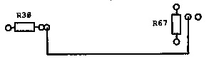 b. cut etch to U73-1 (component side)
cut etch to U74-6 (solder side)
c. jumper U73-1 to U60-7
jumper U74-6 to U74-5
ECN 1007. Purpose: To eliminate double clocking at U156-13
resulting in double vertical display
a. add 220pf ceramic capacitor from U159-12
to U159-14
ECN 1008. Purpose: To eliminate the possibility of heat
damage to board due to heat resulting from CR17.
a. remove the Bridge at CR17 from board
b. mount Bridge on case using case chassis as heat
sink
c. connect the 9VAC outputs from the transformer
directly to the AC inputs of the Bridge
d. connect the "+" output of the bridge to pin 1 of
the female molex connecter that fits on J5 (use
19 gauge wire)
f. connect the "-" output of the bridge to pin 4 of
the female molex connector that fits on J5 (use
19 gauge wire)
g. connect pin 1 of the male molex connector on J5
to the feedthrough marked "+" within the silk-
screened area marked for CR17 (use 19 gauge wire)
ECN 1009. Purpose: to avoid ripple on the -12V supply
due to heat damage to C131 and C125.
a. remove C131 and C125.
b. install a 220 ufd +- 20% 25VDC with the
leg to the "IN" of Q11 and the "+" leg to
gnd.
ECN 1010. Purpose: To improve video stability and to remove
potentiometers at R98, R99, and R129, ther eby
eliminating some of the video adjustments in
the NTSC color video output.
a. Change the following components:
1. R129 from a 10K pot to 4.7K ohms
2. R98 from a 1K pot to 750 ohms
3. R99 from a 1K pot to 750 ohms
4. R124 from 220 to 10 ohms
5. R94 from a 1K pot to a 2.2K pot
6. R109 from 2K to 1.2K ohms
7. C113 from 220pf to 47pf MICA
8. U119 from 74S04 to 74LS19
9. C84 from 100pf to a 10.738MHz CRYSTAL
NOTE: 10-14 ARE OPTIONAL
10. U122 from 74S157 to 74LS157
11. U121 from 74S74 to 74LS74
12. U124 from 74S74 to 74LS74
13. U160 from 74S161 to 74LS161
14. U161 from 74S161 to 74LS161
b. remove the following parts completely
1. C140, L2, R62, R63, and R67
c. install the following
1. 15pf ceramic capacitor from bottom side of
R62 to top side of R63
2. 20K ohms 1/4W 5% from U103-8 to C140 .(left side)
3. 6.8 ufd tant. elect. parallel with R110, with
the "+" side facing C95.
d. cut the etch to U119-12 (solder side).
e. jumper from U1-5 to U103-9.
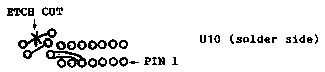
ECN 2000. Purpose: Reduce noise on RAS*, GAS*, RD*, and
MUX and thereby increase memory reliability.
a. Regenerate MUX from RAS*
1. Verify the removal of all termination resisters
on J3, also R68, R69, and C14
2. cut etch near U10 {solder side) such that MUX is
open circuited from U36-13 to J3-16
b. cut etch to U73-1 (component side)
cut etch to U74-6 (solder side)
c. jumper U73-1 to U60-7
jumper U74-6 to U74-5
ECN 1007. Purpose: To eliminate double clocking at U156-13
resulting in double vertical display
a. add 220pf ceramic capacitor from U159-12
to U159-14
ECN 1008. Purpose: To eliminate the possibility of heat
damage to board due to heat resulting from CR17.
a. remove the Bridge at CR17 from board
b. mount Bridge on case using case chassis as heat
sink
c. connect the 9VAC outputs from the transformer
directly to the AC inputs of the Bridge
d. connect the "+" output of the bridge to pin 1 of
the female molex connecter that fits on J5 (use
19 gauge wire)
f. connect the "-" output of the bridge to pin 4 of
the female molex connector that fits on J5 (use
19 gauge wire)
g. connect pin 1 of the male molex connector on J5
to the feedthrough marked "+" within the silk-
screened area marked for CR17 (use 19 gauge wire)
ECN 1009. Purpose: to avoid ripple on the -12V supply
due to heat damage to C131 and C125.
a. remove C131 and C125.
b. install a 220 ufd +- 20% 25VDC with the
leg to the "IN" of Q11 and the "+" leg to
gnd.
ECN 1010. Purpose: To improve video stability and to remove
potentiometers at R98, R99, and R129, ther eby
eliminating some of the video adjustments in
the NTSC color video output.
a. Change the following components:
1. R129 from a 10K pot to 4.7K ohms
2. R98 from a 1K pot to 750 ohms
3. R99 from a 1K pot to 750 ohms
4. R124 from 220 to 10 ohms
5. R94 from a 1K pot to a 2.2K pot
6. R109 from 2K to 1.2K ohms
7. C113 from 220pf to 47pf MICA
8. U119 from 74S04 to 74LS19
9. C84 from 100pf to a 10.738MHz CRYSTAL
NOTE: 10-14 ARE OPTIONAL
10. U122 from 74S157 to 74LS157
11. U121 from 74S74 to 74LS74
12. U124 from 74S74 to 74LS74
13. U160 from 74S161 to 74LS161
14. U161 from 74S161 to 74LS161
b. remove the following parts completely
1. C140, L2, R62, R63, and R67
c. install the following
1. 15pf ceramic capacitor from bottom side of
R62 to top side of R63
2. 20K ohms 1/4W 5% from U103-8 to C140 .(left side)
3. 6.8 ufd tant. elect. parallel with R110, with
the "+" side facing C95.
d. cut the etch to U119-12 (solder side).
e. jumper from U1-5 to U103-9.
ECN 2000. Purpose: Reduce noise on RAS*, GAS*, RD*, and
MUX and thereby increase memory reliability.
a. Regenerate MUX from RAS*
1. Verify the removal of all termination resisters
on J3, also R68, R69, and C14
2. cut etch near U10 {solder side) such that MUX is
open circuited from U36-13 to J3-16
 3. install the following jumpers:
from U36-14 to U20-3
from U36-13 to U20-4
b. Cut etch between the following prints:
1. R34 and R46 (near J3)
2. R35 and 847 (near Jg)
c. Install the following components:
1. 100pf ceramic cap from U36-6 to U36-10
2. 100pf ceramic cap from U36-15 to U36-10
3. 330pf ceramic cap from U36-8 to U36-10
4. 75 ohm resistor from R34 to R46
5. 75 ohm resistor from 835 to R47
d. Use J3 when connecting from the main computer to
the expansion board
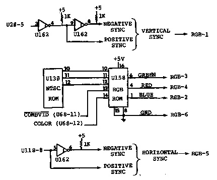
RGB OPTION
The following components and jumpers must be installed
to obtain the RGB video output.
A. INSTALL THE FOLLOWING COMPONENTS
RGB VIDEO CONNECTOR- 6 pin din jack
U131- 74LS257
U132- 74LS174
U158- RGB ROM
C146- 680 pf ceramic cap(from U129-1 to U129-8)
B. INSTALL THE FOLLOWING JUMPERS
1. USE 24 GAUGE STRANDED WIRE TO CONNECT TO RGB
6 PIN DIN JACK
U162-9 TO RGB-1* VERTICAL SYNC
U158-l TO RGB-2 BLUE
U158-6 TO RGB-3 GREEN
U158-4 TO RGB-4 RED
U162-5 TO RGB-5* HORIZONTAL SYNC
U158-8 TO RGB-6 GROUND
2. USE 30 GAUGE NON-STRANDED WIRE
U20-5 TO U162-3
U118-8 TO U162-5
U162-4 TO U162-9
U68-12 TO U158-14
U68-11 TO U158-13
U130-12 TO U158-12
U130-11 TO U158-11
U130-18 TO U158-18
U158-15 TO U158-8
C. INSTALL THE FOLLOWING RESISTORS
1K ohms from U162-4 to U162-14
1k ohms from U162-6 to U162-14
1k ohms from U162-8 to U162-14
* Note that factory built LNW80's are set up for both
positive horizontal and vertical syncs. Negative sync pulses
may be obtained by moving the following jumpers:
RGB-1 from UX62-9 to U162-8
RGB-5 from U162-5 to U162-6
Because U162 has open collector gates, a combined negative
sync may be obtained by setting up for negative syncs and then
connecting the sync outputs together.
Because the RGB ROM also has open collector gates it may be
necessary to install 330 ohm pull-up resistors on it's
outputs, pins 1, 4, and 6. Note that this is only necessary
with monitors that do not internally pull up the RED, GREEN,
and BLUE lines. This is not necessary with the ANDEC COLOR II
RGB MONITOR.
RGB CIRCUIT LOGIC DIAGRAM
3. install the following jumpers:
from U36-14 to U20-3
from U36-13 to U20-4
b. Cut etch between the following prints:
1. R34 and R46 (near J3)
2. R35 and 847 (near Jg)
c. Install the following components:
1. 100pf ceramic cap from U36-6 to U36-10
2. 100pf ceramic cap from U36-15 to U36-10
3. 330pf ceramic cap from U36-8 to U36-10
4. 75 ohm resistor from R34 to R46
5. 75 ohm resistor from 835 to R47
d. Use J3 when connecting from the main computer to
the expansion board
RGB OPTION
The following components and jumpers must be installed
to obtain the RGB video output.
A. INSTALL THE FOLLOWING COMPONENTS
RGB VIDEO CONNECTOR- 6 pin din jack
U131- 74LS257
U132- 74LS174
U158- RGB ROM
C146- 680 pf ceramic cap(from U129-1 to U129-8)
B. INSTALL THE FOLLOWING JUMPERS
1. USE 24 GAUGE STRANDED WIRE TO CONNECT TO RGB
6 PIN DIN JACK
U162-9 TO RGB-1* VERTICAL SYNC
U158-l TO RGB-2 BLUE
U158-6 TO RGB-3 GREEN
U158-4 TO RGB-4 RED
U162-5 TO RGB-5* HORIZONTAL SYNC
U158-8 TO RGB-6 GROUND
2. USE 30 GAUGE NON-STRANDED WIRE
U20-5 TO U162-3
U118-8 TO U162-5
U162-4 TO U162-9
U68-12 TO U158-14
U68-11 TO U158-13
U130-12 TO U158-12
U130-11 TO U158-11
U130-18 TO U158-18
U158-15 TO U158-8
C. INSTALL THE FOLLOWING RESISTORS
1K ohms from U162-4 to U162-14
1k ohms from U162-6 to U162-14
1k ohms from U162-8 to U162-14
* Note that factory built LNW80's are set up for both
positive horizontal and vertical syncs. Negative sync pulses
may be obtained by moving the following jumpers:
RGB-1 from UX62-9 to U162-8
RGB-5 from U162-5 to U162-6
Because U162 has open collector gates, a combined negative
sync may be obtained by setting up for negative syncs and then
connecting the sync outputs together.
Because the RGB ROM also has open collector gates it may be
necessary to install 330 ohm pull-up resistors on it's
outputs, pins 1, 4, and 6. Note that this is only necessary
with monitors that do not internally pull up the RED, GREEN,
and BLUE lines. This is not necessary with the ANDEC COLOR II
RGB MONITOR.
RGB CIRCUIT LOGIC DIAGRAM
 TOC | Next Page